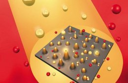
Semiconductor nanostructures for Optoelectronic Devices
To grow the ZnO NRAs on silica microspheres, we layered aluminum-doped ZnO (AZO) as a seed layer over the surface of microspheres by radio-frequency magnetron sputtering…
Nanostructures of ZnO
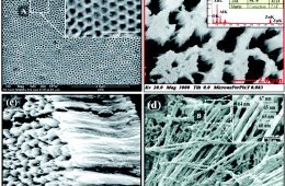
The scanning electron microscopy images of TZO products in Fig. 2a reveal that TiO2 NPs with diameters in the range of 20–250nm are deposited on one of the frontier…
Evolution of Gold nanostructures on Graphene

Department of Engineering Physics, McMaster University, Hamilton Ontario, Canada L8S 4L7, Brockhouse Institute for Materials Research, McMaster University, Hamilton…
Optical response of nanostructures

Invisibility cloak and gravitational control using nonlinear optics and morphogenetic technology V.Grebennikov Metamaterials Electromagnetic metamaterials are…
Heterogeneous nanostructures

Astronomy Biomedical Optics & Medical Imaging Defense & Security Electronic Imaging & Signal Processing Illumination & Displays Lasers…
Engineering carbon nanostructures with electrons
†National Institute of Advanced Industrial Science and Technology, 1-1-1 Higashi, Tsukuba, Ibaraki 305-8566, Japan ‡Tokyo Institute of Technology, 4259 Nagatsuta-cho…
Nanostructures in quantum computation

Papers and Full Proposals may be submitted and received at any time until the final BAA deadline of 4:00PM ET, September 8, 2008. 1. The Mathematics of the Brain…
Journal of Nanostructured

Oct. 2006: President George W. Bush signed the Department of Defense Authorization legislation. The House amendment was authored and introduced by Rep. Jim McDermott…
Nanostructures Self Assembly

MIT has devised a way of creating complex, self-assembling 3D nanostructures of wires and junctions. While self-assembling structures have been made from polymers…