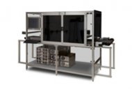
 Xenon Corporation’s Printed Electronics Testing Network Offers Expertise in Wide Range of PE Disciplines
By David Savastano
Entrepreneurs working on new projects utilizing printed electronics can find the process daunting. Often, they are matching new substrates and materials, and the choice of a manufacturing process in itself is challenging, as there is a huge difference between R&D and production.
To help these innovators navigate the many challenges they face, a group of companies and universities have formed the Printed Electronics Testing Network (PETN). Formed by Xenon Corporation, this network is offering companies and universities the opportunity to come into their facilities, learn if their applications will work and offer advice on possible improvements.
The goal of the Printed Electronics Testing Network is to support research and development, share knowledge across the network, and through these efforts, to advance the practical use of printed electronics in commercial applications.
“Our past business models have shown that by working closely on a global basis with critical technologies required for achieving successful R&D for emerging markets, one can establish test centers that can expedite proof of concept in a relatively short time at a very cost effective approach, ” said Louis Panico, CEO at Xenon Corporation.
“The Printed Electronics Testing Network immediately provides a technical collaboration of multi-formulation, dispensing companies and integrators with high energy ‘pulsed light’ sources for addressing key issues of PE process development and manufacturability, ” Panico added.
The PETN members have a wide range of disciplines, beginning with Xenon Corporation’s sintering capabilities, which convert the printed ink layer into a solid uniform layer of conductive material through the use of pulsed light, as well as inks, printers and more.
“Xenon’s strongest capability is providing the equipment and technology for “Pulsed Light” sintering of metallic inks for the printed electronic markets, ” Panico said. “Xenon brings five decades of experience in “Pulsed Light” technology to facilitate the development and manufacturability of printed electronics products. We have thousands of pulsed light systems operating 24/7 on worldwide production lines.”
 Xenon’s sintering systems are available at all of the PETN facilities. Companies interested in joining the PETN can contact Xenon, and those who are interested in testing can contact Xenon at LAPanico@xenoncorp.com.
“We are seeing an abundance of requests for the Testing Network from end-users and machine makers, ” Panico said. “The quantity of application testing requests is growing exponentially. The biggest challenge is bringing the printed electronics market from the R&D stage to meeting the needs of a variety of R2R processes, specifically substrate adhesion and metallic ink thickness.”
Intrinsiq Materials manufactures nanoparticle-based screen and inkjet inks. Dr. Sujatha Ramanujan, chief operating officer for Intrinsiq Materials, said there is a lot to consider when it comes to developing printed electronics applications.


