 Direct visualisation of the magnetic structure of materials is exciting not only from a fundamental physics perspective, but is also critical for proposed spintronic applications. As a research group, we have a long history and associated extensive publication track record in magnetic imaging by Lorentz transmission electron microscopy (TEM). The advent of a new JEOL ARM-200cF TEM has placed us in a world-leading position in terms of our magnetic imaging capabilities, and we recently demonstrated a spatial resolution of ~1 nm.
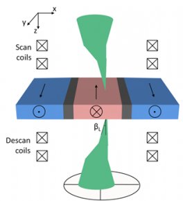
Lorentz microscopy relies on small deflections of electrons on passing through a magnetic specimen. These deflections are the result of the Lorentz force and are used to generate contrast in the image. In one mode of Lorentz microscopy, known as differential phase contrast (DPC) imaging, the beam is focused to a probe and scanned across the specimen. pposite quadrants, a pair of magnetic induction maps is generated.
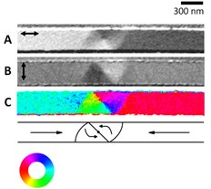
This is illustrated in the figure, which shows typical results collected from a magnetic vortex domain wall in a Ni80Fe20 nanowire. Images A and B are orthogonal induction maps where the arrows indicate the direction of sensitivity. Further analysis of the image pair yields a quantitative vector map of magnetic induction, given by C. The colour map vividly shows the detailed internal structure of the domain wall.
[1] J. N. Chapman, J. Phys. D: Appl. Phys., 17 623 (1984).
[2] S. McVitie and M. Cushley, Ultramicroscopy 106, 423 (2006).
[3] S. McVitie, G. S. White, J. Scott, P. Warin and J. N. Chapman, J. Appl. Phys. 90, 5220 (2001).
 The following Lorentz images were acquired using a Philips CM20 FEG TEM and further illustrates the variety of magnetic systems we work on.
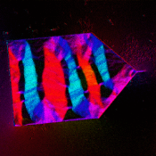
Differential phase contrast image of a multilayer NiFe/CoFe/Al2O3/NiFe/CoFe film patterned into a magnetic recording head-like geometry. Dark regions indicate zero net magnetic induction.
X. Kong et al., J. Appl. Phys. 104, 013925 (2008).

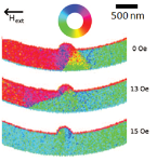
De-pinning of a transverse domain wall from a deliberately fabricated pinning site, or notch.
Cross-tie density strongly increases with reduced element width as observed in these NiFe elements.N. Wiese et al., E. Phys. Lett 80, 57003
The ability to precisely control the motion of magnetic domain walls in ferromagnetic nanowires is crucial for the future realization of proposed spintronic devices. We have created non-topographic domain wall pinning sites using the FIB to locally modify the magnetic properties of the material. The figure below illustrates a FIB induced change in magnetic induction in a NiFe film using a dose of 8 x 10¹⁵ ions/cm2; calculations indicate a 50% reduction of the saturation magnetisation in the irradiated region.


