 The wave nature of light expresses itself in the propagation all over space, showing an intrinsic limitation to be localized beyond the so-called diffraction limit which is of the order of half the wavelength of the photons propagating. However when interacting with matter, light often gets reflected, diffracted, scattered or absorbed depending on the interactions and excitations induced in the material.
 engths, between 450 nm and 800 nm, metals interact with electromagnetic waves producing a variety of optical effects. The conduction electrons that constitute the metal can oscillate rigidly at certain optical frequencies that depend on the electron density. Furthermore, when metals are physically bounded by surfaces and interfaces as it is usually the case in nanoparticles and nanostructures, the oscillations of the electron charge density at the surfaces show resonant localized modes so-called surface plasmons. The excitation of these surface plamons by light produces a localization and enhancement of the visible light at the surface of the metal at distances of a few nanometers, well below the diffraction limit, thus acting metallic nanostructures as resonant emitters or receptors of light. This is the reason why metallic nanostructures are often referred to as optical nanoantennas.
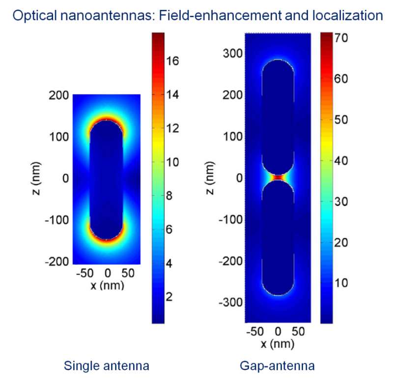
![Fig. 4. (a) Extinction cross section and (b) near-field enhancement at the gap of two metallic nanoparticles as a function of separation distance between the particles calculated within a classical formalism. (c) and (d) show the same calculation as in (a) and (b) with use of a quantum-corrected model [3] to describe the interaction between nanoparticles. The differences of the results between the two approaches are clear both in the far-field as well as in the near-field.](/img/fullsize/fig_4_a_extinction_cross_section_800x601.png) An example of the simplest optical nanoantenna one can think of is shown in Fig. 1a. A metallic nanoparticle enhances both the absorption and the scattering of visible light acting as an isotropic optical nanoantenna. The spectrum of scattering and emission (Fig.1b) shows a distinctive resonance or antenna mode sustained by the excitation of localized surface plasmons.
An example of the simplest optical nanoantenna one can think of is shown in Fig. 1a. A metallic nanoparticle enhances both the absorption and the scattering of visible light acting as an isotropic optical nanoantenna. The spectrum of scattering and emission (Fig.1b) shows a distinctive resonance or antenna mode sustained by the excitation of localized surface plasmons.
In the last years, the development of sophisticated fabrication techniques that range from electron beam lithography to wet chemistry synthesis, together with the improvement of optical characterization techniques allowing for accessing far-field as well as near-field properties in the nanoscale have made possible to study ultrafast processes and nonlinear phenomena induced by intense light pulses. In parallel, new theoretical frameworks have been developed to describe the main features of the complex physical processes involved in the interaction between light and matter, boosting tremendously the field of plasmonics .


